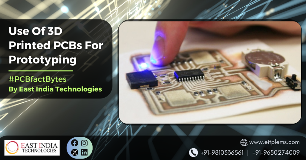
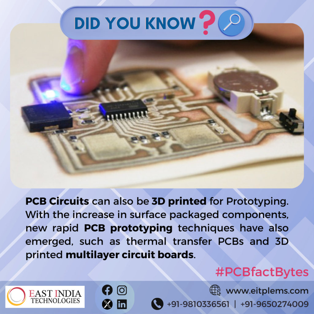
Tests on circuits can be carried out locally with the aid of breadboards, cavities boards, and other all-purpose circuit boards. However, new quick PCB (Printed Circuit Board) prototype techniques have also evolved, such as thermal transfer PCBs and 3D printed multilayer PCBs, in response to the rise in surface packaged components and the requirement for compact and complicated designs. In this essay, we will examine the advantages, uses, and prospective effects of 3D printed PCBs for prototyping in the electronics sector.
The Development of 3D-Printed PCBs
While effective, conventional PCB prototype techniques frequently have drawbacks, particularly when it comes to quick design revisions and the incorporation of three-dimensional components. Here is where the field is starting to change thanks to 3D printed PCBs. As of now, 3D Printed PCBs are mostly used in prototypes because the researchers can 3D print just a few samples (even a single sample) for their prototyping needs & its the prototype fails, it is very easy to make changes in the design file & start over again with less efforts.
Applications of 3D Printed PCBs
- Consumer Electronics: 3D printed PCBs are finding applications in consumer electronics, allowing manufacturers to create compact and aesthetically pleasing designs. This is particularly beneficial for wearables, smartphones, and IoT devices.
- Medical Devices: The healthcare industry is benefiting from 3D printed PCBs, which enable the development of smaller and more portable medical devices. These PCBs can be customized to fit into specialized equipment or implants.
- Aerospace and Defense: In aerospace and defense, where weight and space constraints are critical, 3D printed PCBs are used to create lightweight, yet robust, circuitry for various applications, including drones and satellite systems.
- Automotive: Automotive manufacturers are leveraging 3D printed PCBs to enhance the functionality and aesthetics of vehicle interiors while reducing weight and improving overall performance.
- Research and Education: 3D printed PCBs are also valuable in educational and research settings, enabling students and researchers to quickly iterate and experiment with new electronic designs.
Challenges and Future Outlook
While 3D printed PCBs offer numerous advantages, they are not without challenges. Material selection, conductivity, and thermal properties are critical considerations. However, ongoing research and development efforts are addressing these issues, paving the way for broader adoption.
In conclusion, 3D printed PCBs are transforming the world of electronics prototyping. The ability of 3D Printed PCBs to accommodate complex designs, high customization, and rapid prototyping capabilities make them an invaluable tool for engineers and designers across various industries. As technology continues to advance, we can expect 3D printed PCBs to play an increasingly significant role in shaping the future of electronics innovation.
Follow us & subscribe to our newsletter/blogs to stay updated with the latest trends in the PCB & SMT industry. More such facts and news get updated on our blogs/articles every week.
We are East India Technologies Pvt Ltd, one of the leading PCB assembly & SMT / EMS service providers in India. For any of your EMS needs, you can reach out to us at info@eitpl.com or dial us at +919650274009 . We are available every Monday to Saturday. We serve our clients not only in India but across the globe as well.